магазин
wafer fabrication process flow chart
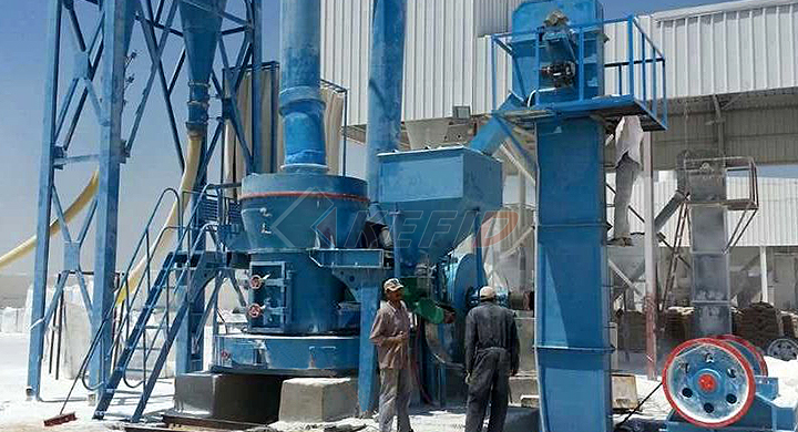
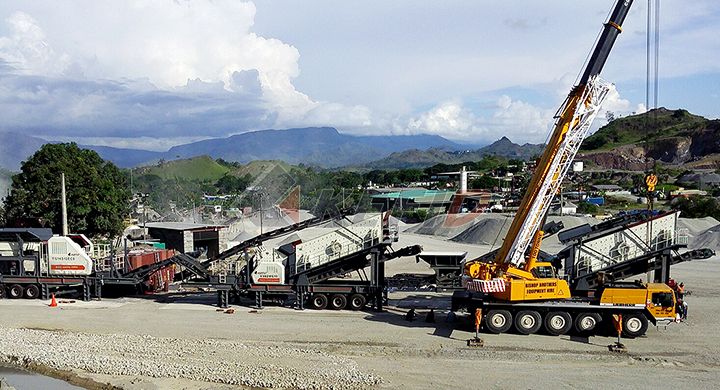
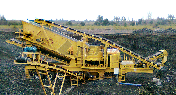
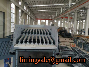
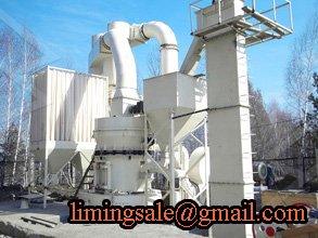
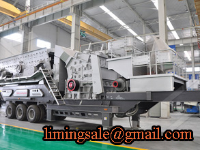
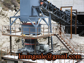
KEFID,Дробильно-сортировочное оборудование Китая высокого качества, стандартное дробильное оборудование. На протяжении более 30 лет мы занимаемся исследованиями и разработками и производством дробильного оборудования, дробления зданий, промышленных дробилок и экологически чистых строительных материалов, и предлагаем профессиональные решения и дополнительные продукты для создания ценность для клиентов.


Онлайн сообщение
wafer fabrication process flow chart
Wafer Manufacturing | How Are Semiconductors Made?
Wafer Fabrication The most important step in the manufacturing process is the fabrication of the wafer This is where the integrated circuit is formed in and on the wafer The fabrication process, which takes place in a clean room, involves a series of steps and the process can take anywhere from 10 to 30 days to completeManufacturing Flow Chart of an Integrated Circuit 11 WAFER FABRICATION (FRONTEND) Identical integrated circuits, called die, are made on each wafer in a multistep process Each step adds a new layer to the wafer or modifies the existing one These layers form the elements of the individual electronic circuits The main steps for theAN900 APPLICATION NOTE STMicroelectronics
Eight Major Steps to Semiconductor Fabrication, Part 1
The largest wafer diameter used in semiconductor fabrication today is 12 inches, or 300mm Smoothing things out – the lapping and polishing process Sliced wafers need to be prepped before they are productionready Abrasive chemicals and machines polish the uneven surface of the wafer25 Fabrication 251 Description of Semiconductor Manufacturing Processes In the following subsections an overview over the different process steps, a wafer undergoes during its fabrication in the cleanroom, is given A semiconductor manufacturing process25 Fabrication
1 Semiconductor manufacturing process : Hitachi HighTech
In the manufacturing process of IC, electronic circuits with components such as transistors are formed on the surface of a silicon crystal wafer Basics of IC formation A thin film layer that will form the wiring, transistors and other components is deposited on the wafer (deposition) The thin film is coated with photoresist The circuit pattern of the photomask (reticle) is then projectedWafer Fabrication Data Analog Devices has a very active reliability monitoring and prediction program to ensure all products shipped by ADI are of the highest quality ADI conducts all major classes of reliability tests on each of its processes utilizing state of the art equipment and methodologiesWafer Fabrication Data | Analog Devices
Process Flow Chart – Bumping
Process Flow Chart – Bumping (Wafer is cleaned before each individual process step) Photoresist Masking: • Photoresist Spinning and Baking • Mask Alignment and Exposure • Photoresist Development Electrochemical Plating: • UBM 3 • Bump Metal 1 • Bump Metal 2 Field Metallization Sputtering:Oct 06, 2017· Back End(BE) Process Wafer Back Grinding • The typical wafer supplied from ‘wafer fab’ is 600 to 750μm thick • Wafer thinned down to the required thickness, 50um to 75um, by abrasive grinding wheel › 1st step : Use a large grit to coarsely grind the wafer and remove the bulk of the excess waferIntroduction to Semico nductor Manufacturing and FA Process
Wafer : The Complete Production Process Discover Food Tech
Nov 06, 2016· The baking process involves the usage of Wafer Ovens Ovens are made up of heated metal plates hinged at one side, typically thin and usually bear intricate surface patterns The plate pairs either attached to heavy carriers or are selfsupporting linked together to form a chainthe wafer fabrication process parameters and thus to the potential physical defects that might occur 2) SRAM/DRAM/Flash/Analog Product Testing Flow The templates of Commercial SRAM, DRAM, Flash, Analog TEST Flow & Control are shown in Figures 33, 34 35 and 36 respectively 3) Known Good Die Testing FlowQuality Assurance in the Project Approval Stage
semiconductor manufacturing process flow chart
wafer fabrication, is the extremely sophisticated and intricate process of manufacturing the silicon chip Manufacturing Flow Chart of an Integrated Circuit Get price25 Fabrication 251 Description of Semiconductor Manufacturing Processes In the following subsections an overview over the different process steps, a wafer undergoes during its fabrication in the cleanroom, is given A semiconductor manufacturing process25 Fabrication
Wafer : The Complete Production Process Discover Food Tech
Nov 06, 2016· The baking process involves the usage of Wafer Ovens Ovens are made up of heated metal plates hinged at one side, typically thin and usually bear intricate surface patterns The plate pairs either attached to heavy carriers or are selfsupporting linked together to form a chainNew Jersey Institute of TechnologyNew Jersey Institute of Technology
wafer fabrication process flow chart ScalepaintDiorama`s
THE MANUFACTURING PROCESS n Overview of manufacturing process n Design rules n chapter2fm Page 33 Monday, September 4, 2000 11:11 AM 34 THE MANUFACTURING PROCESS Chapter 2 221 The Silicon Wafer The base material for the manufacturing process comes in the form of a singlecrystalline, Read moreOct 09, 2014· CMOS Fabrication Process / Cmglee / CC BY SA A modern wafer will undergo this process around 50 times or so before creating the final finished chipManufacturing: From Wafer to Chip An Introduction to
chapter2fm Page 33 Monday, September 4, 2000 11:11 AM
repetitively in the course of the manufacturing process Rather than diving directly into a description of the overall process flow, we first discuss the starting material followed by a detailed perspective on some of the mostoften recurring operations 221 The Silicon Wafer The base material for the manufacturing process comesAug 19, 2014· Wafer manufacturing process 1 Semiconductor Manufacturing Process Fundamental Processing Steps: 1Silicon Manufacturing a) Czochralski method b) Wafer Manufacturing c) Crystal structure 2Photolithography a) Photoresists b) Photomask and Reticles c) Patterning 2Wafer manufacturing process LinkedIn SlideShare
Wafer fabrication Wikipedia
Wafer fabrication is a procedure composed of many repeated sequential processes to produce complete electrical or photonic circuits on semiconductor wafersExamples include production of radio frequency amplifiers, LEDs, optical computer components, and CPUs for computersWafer fabrication is used to build components with the necessary electrical structuresOct 09, 2014· Sil'Tronix Silicon Technologies manufactures silicon wafers Here is the full process Sil'Tronix Silicon Technologies fabrique des wafers de silicium Voici le procédé wwwsiltronixstWafer manufacturing process
Fabrication process flow: Basic steps
Jan 14, 2018· Lithography, Negative photo resist material, Positive Photo resist material,Shop popular waferfabricationprocessflowchart chosen by Drop communities Join Drop to discover the latest details on Aurender Flow DAC/Amp, Nike FlowShop Wafer Fabrication Process Flow Chart & Discover

FUJITSU SEMICONDUCTOR LIMITED Quality and Reliability
• Example of Quality Control Flowchart • Incoming Inspection • InProcess Inspections • InProcess QA Inspection 14 • Statistical Process Control (SPC) 15 Maintaining the Quality and Reliability of Semiconductor Devices 16 Quality and Reliability Support • Equipment Maintenance • Measurement System Analysis (MSA) 16Oct 09, 2015· This is achieved by printing the metal pastes with special screen printing devices that place these metal inlines onto the backside After printing, the wafer undergoes a drying process Once dry, this process is followed by the printing of the front side contacts, then the wafer is another time dried After all contacts have been printed on the rear and front sides, the screenprinted wafersSolar Cell Production: from silicon wafer to cell
Wafer manufacturing process LinkedIn SlideShare
Aug 19, 2014· Wafer manufacturing process 1 Semiconductor Manufacturing Process Fundamental Processing Steps: 1Silicon Manufacturing a) Czochralski method b) Wafer Manufacturing c) Crystal structure 2Photolithography a) Photoresists b) Photomask and Reticles c) Patterning 2THE MANUFACTURING PROCESS n Overview of manufacturing process n Design rules n chapter2fm Page 33 Monday, September 4, 2000 11:11 AM 34 THE MANUFACTURING PROCESS Chapter 2 221 The Silicon Wafer The base material for the manufacturing process comes in the form of a singlecrystalline, Read morewafer fabrication process flow chart ScalepaintDiorama`s
Basics of Semiconductor and Process flowchart; Video on
Semiconductor Packaging Overview : Basics of Semiconductor and Process flowchart; Video on SandtoSilicon Wafer fabrication, inspection and testing Wafer packaging; Packaging evolution; Chip connection choices Wire bonding, TAB and flipchip1 Wire bonding, TAB and flipchip2; TutorialsOct 09, 2014· Sil'Tronix Silicon Technologies manufactures silicon wafers Here is the full process Sil'Tronix Silicon Technologies fabrique des wafers de silicium Voici le procédé wwwsiltronixstWafer manufacturing process
Fabrication and Manufacturing (Basics)
Fabrication Steps • Features are patterned on a wafer by a photolithographic process – Photolight lithography, n process of printing from a plane surface on which image to be printed is inkreceptive and the blank area is inkrepellant • Cover the wafer with a lightsensitive, organic material called photoresistdesired After briefly discussing the wafer production process and the operational planning and control issues in wafer manufacturing and fabrication, current state of research is introduced Subsequently, several plausible and fruitful directions for future research are outlined 2 The wafer production Manufacturing of semiconductors startsOperational planning and control of semiconductor wafer
Solar Cell Production: from silicon wafer to cell
Oct 09, 2015· This is achieved by printing the metal pastes with special screen printing devices that place these metal inlines onto the backside After printing, the wafer undergoes a drying process Once dry, this process is followed by the printing of the front side contacts, then the wafer is another time dried After all contacts have been printed on the rear and front sides, the screenprinted wafersThe given n type silicon wafer is a unpolished one So polishing is required and is done by 20 % NAOH solution at temperature 85O C for 3 to 5 minutes C) Wafer Cleaning Wafer cleaning is a very important step in device fabrication process because of the variety of organic and inorganic contaminants of unknown origin, which areFABRICATION AND CHARACTERIATION OF PN JUNCTION
SiC Chip Demand Surges Semiconductor Engineering
SiC requires a selective annealing process “For power devices, the current flow is through the wafer You need a good electrical conduction with the metal interface,” said HansUlrich Zühlke, product manager at 3DMicromac “We only heat up the backside of the wafer to anneal the Ohmic contact to make a metal silicon carbide interface”• Example of Quality Control Flowchart • Incoming Inspection • InProcess Inspections • InProcess QA Inspection 14 • Statistical Process Control (SPC) 15 Maintaining the Quality and Reliability of Semiconductor Devices 16 Quality and Reliability Support • Equipment Maintenance • Measurement System Analysis (MSA) 16FUJITSU SEMICONDUCTOR LIMITED Quality and Reliability
CMOS Fabrication : Process Steps And Twin tub Process
Sep 24, 2019· In early 1960’s the semiconductor manufacturing process was initiated from Texas and in 1963 CMOS or complementary metal oxide semiconductor was patented by Frank Wanlass Integrated circuits are manufactured by utilizing the semiconductor device fabrication process These ICs are major components of every electrical and electronic devices which we use in our daily lifeThe Process: The fabrication process can be broken up into five simple steps Below is a flow chart of these steps followed by a short description of what each step should accomplish Clicking on the flow chart will take you to a link with the all steps required to build an accelerometerMEMS Fabrication Montana State University
USB2 Semiconductor wafer manufacturing method
The present invention provides a method for manufacturing a semiconductor wafer capable of manufacturing a wafer without ringlike sag in an outer peripheral portion thereof when polishing an alkali etched wafer, and a wafer without the ringlike sag in an outer peripheral portion thereof The present invention comprises: a back surface part polishing and edge polishing step for performingThe growing process is very automated and yields quality crystals The growth process is very slow, typically 05 inch per hour for 150mm diameter crystals Because of slow growth rates, the manufacturing process consumes large quantities of electricity After the growing process is completed, the silicon ingot is evaluated for both electrical andBASIC INTEGRATED CIRCUIT MANUFACTURING