магазин
crushing machine for wafer die common failures
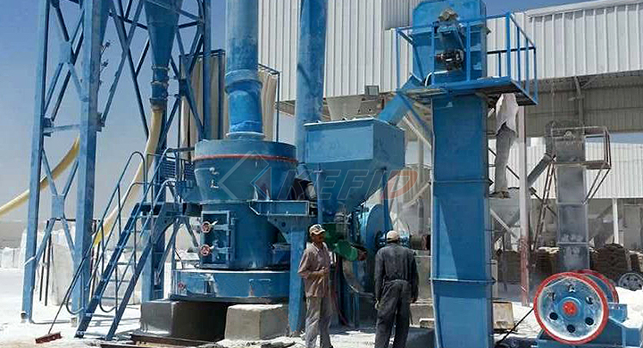
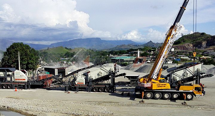
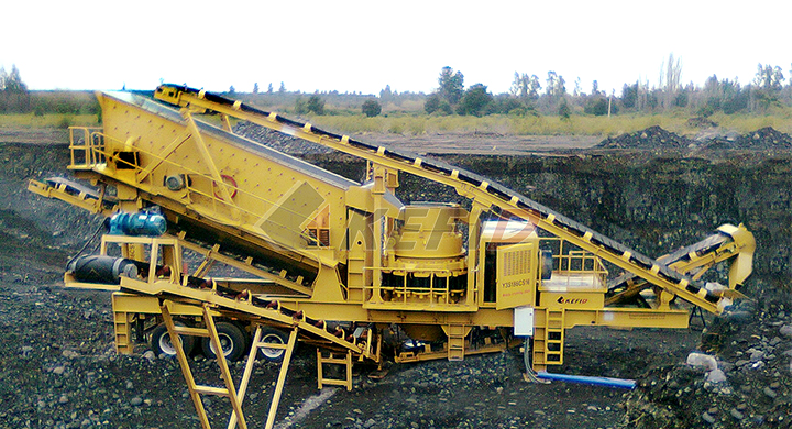
KEFID,Дробильно-сортировочное оборудование Китая высокого качества, стандартное дробильное оборудование. На протяжении более 30 лет мы занимаемся исследованиями и разработками и производством дробильного оборудования, дробления зданий, промышленных дробилок и экологически чистых строительных материалов, и предлагаем профессиональные решения и дополнительные продукты для создания ценность для клиентов.
Онлайн сообщение
crushing machine for wafer die common failures
WAFER WITH DIE MAP Texas Instruments Incorporated
May 19, 2016· At each die location, the die is picked and placed if it is a known good die, based on the wafer map, or it is left if it is a known defective die, based on the wafer map After picking all of the known good die, the wafer table is again stepped to the location that is believed to be the reference die, as indicated by track 114 If theAug 14, 2018· World Dangerous Machine Destroys Everything, Powerful Rock Crusher And Tire Shredding Machine Shredder Bulky Waste And Oil Filter Recycling, Solid Bulky WasteWorld Dangerous Machine Destroys Everything, Powerful Rock

silicon wafer edge grinding
A Study of Grinding Marks in Semiconductor Wafer Grinding development for wafer grinding but cannot be applied directly Fig 1 shows the setup of wafer grinding The grinding wheel is modeled as a single point cutter and it removes the work material from the edge to the center along the curve MO as shown in Fig 2 Two coordinate systems are used to define all the points on the wafer andJun 30, 2019· Crazy Dangerous Fast Skills Car Crusher Machine Destroys Everything Modern Technology Duration: 11:02 KenTT 751,633 views 11:02 Satisfactory Machine Cutting And BendingThe Crusher Destroy Everything Process is Amazing
Identifying the Cause of Tool and Die Failure
Jan 06, 2016· Machining problems are a common cause of tool and die failures It is generally best to avoid machining directly to the finish size unless prehardened die steels are used Obtaining perfect control of surface chemistry and size during heat treatment is difficult Thus, some final grinding is usually needed after heat treatmentIntroduction To Die & Wafer Products SBOA147 factors, such as the cost of the substrate and efficiency of the rework process machine, or process in which TI components or services are used Information anticipate dangerous consequences of failures, monitor failures and their consequences, lessen the likelihood of failures that mightDie & Wafer Overview Texas Instruments
The Ultimate Guide to Wafer Sort AnySilicon
Jan 25, 2017· Wafer sort’s main purpose is to identify the nonfunctional dies and thereby avoiding assembly of those dies into packages In many cases, wafer sort is a simple and quick test that focuses on a few electrical parameters that are most likely to fail Wafer testing is performed during IC production on every wafer and every silicon dieThe wafer saw process cuts the individual die from the wafer leaving the die on the backing tape The wafer saw equipment consists of automated handling equipment, saw blade, and an image recognition system The image recognition system maps the wafer surface to identify the areas to be cut, known as the saw street DI Water is dispensed onSemiconductor Packaging Assembly Technology

Solution of the common failure of the diecutting machine
Diecutting machine in daily use in the production process will often encounter a variety of failures, this production would have been affected The following aspects of the common failure of the diecutting machine analysis, and provides a solution: 1carton die cutting machine indentation to generate a burst line and dark line The cause of the problem: burst line refers to the die cuttingThe wafer saw process cuts the individual die from the wafer leaving the die on the backing tape The wafer saw equipment consists of automated handling equipment, saw blade, and an image recognition system The image recognition system maps the wafer surface to identify the areas to be cut, known as the saw street DI Water is dispensed onSemiconductor Packaging Assembly Technology
Failure Analysis of Cracked Die ResearchGate
The failure analysis technique of cracked die in microelement was presented in detail, and the cause of these failure components was found finally Wafer processing defect on the die has proven toIn the context of manufacturing integrated circuits, wafer dicing is the process by which die are separated from a wafer of semiconductor following the processing of the wafer The dicing process can involve scribing and breaking, mechanical sawing (normally with a machine called a dicing saw) or laser cuttingAll methods are typically automated to ensure precision and accuracyWafer dicing Wikipedia
The Most Common Accidents in the Mining Industry
Jan 14, 2019· The yearly average in coal mining decreased to 30 fatalities from 20012005, though 60 to 70 miners still die each year in the US coal and noncoal mining industry The most common accidents occurring in the mining industry are the result of poisonous or explosive gases or mishaps relating to the use of explosives for blasting operationsThank you it is direct simple, it will help many to understand common failure types If you add something about mechanism of failure and how to prevent their reoccurrences it will be great Reply Christoffer Wesley says June 4, 2018 at 11:42 am Hi, always nice with some “back to Basics” articles!Failure Modes: Understand the 5 most common failure types

Most Common Causes of Printed Circuit Board Failure
MOST COMMON CAUSES OF CIRCUIT BOARD FAILURE Printed circuit boards, or PCBs, are the driving forces behind almost everything we use today—smart phones, control panels for industrial machines, the display screens at fast food restaurants When a PCB fails, it disrupts both our personal and business livesFigure 6 Description of the Wafer Probing Operation The bad die are automatically marked with a black dot so they can be separated from the good die after the wafer is cut A record of what went wrong with the nonworking die is closely examined by failure analysis engineers to determine where the problem occurred so that it may be correctedAN900 APPLICATION NOTE STMicroelectronics
Injection Molding Process, Defects, Plastic
Injection molding is the most commonly used manufacturing process for the fabrication of plastic parts A wide variety of products are manufactured using injection molding, which vary greatly in their size, complexity, and applicationDie Attach Process Die Attach (also known as Die Mount or Die Bond) is the process of attaching the silicon chip to the die pad or die cavity of the support structure (eg, the leadframe) of the semiconductor packageThere are two common die attach processes, ie, adhesive die attach and eutectic die attachDie Attach, Die Mount, or Die Bond
A ReExamination of Failure Analysis and Root Cause
By contrast, the root cause of a failure is a process or procedure which “went wrong” The finish on a machine part was not asspecified The heattreatment on a rail was not uniform The angle on screwthreads was too steep Identification of that process is the key to creating a procedure by which future failures can be avoidedThe largest wafer diameter used in semiconductor fabrication today is 12 inches, or 300mm Smoothing things out – the lapping and polishing process Sliced wafers need to be prepped before they are productionready Abrasive chemicals and machines polish the uneven surface of the waferEight Major Steps to Semiconductor Fabrication, Part 1

R Crusher Wear Parts Reference Guide
crusher tools EG Jaw liners are subject to numerous pressure and impact stresses Several other factors affect the wear lifetime of crusher wear parts as listed in below Diagram Wear occurs in all crushers , however wear costs can be controlled by selecting the correct crusher type for the abrasive content of the material to be crushedStarring is a common structural defect that appears as a collapse near the core of the roll Caused by uneven stress distribution inside the roll, the starring or collapse of paper is initiated once a portion of the roll, which is wound with a low woundin tension, increases and a ring or hoop of tightly wound paper causes a collapse of thePaper Defects and Defects in Paper
(PDF) Tablet manufacturing processs and defects of tablets
A 'read' is counted each time someone views a publication summary (such as the title, abstract, and list of authors), clicks on a figure, or views or downloads the fulltextMOST COMMON CAUSES OF CIRCUIT BOARD FAILURE Printed circuit boards, or PCBs, are the driving forces behind almost everything we use today—smart phones, control panels for industrial machines, the display screens at fast food restaurants When a PCB fails, it disrupts both our personal and business livesMost Common Causes of Printed Circuit Board Failure
Failure Analysis of Cracked Die ResearchGate
The failure analysis technique of cracked die in microelement was presented in detail, and the cause of these failure components was found finally Wafer processing defect on the die has proven toThe largest wafer diameter used in semiconductor fabrication today is 12 inches, or 300mm Smoothing things out – the lapping and polishing process Sliced wafers need to be prepped before they are productionready Abrasive chemicals and machines polish the uneven surface of the waferEight Major Steps to Semiconductor Fabrication, Part 1
Top Most Satisfying Factory Machines And Ingenious Tools
Mar 31, 2019· Top Most Satisfying Factory Machines And Ingenious Tools Excellent Automatic Machinery Thanks for visiting Support and comment below theFigure 6 Description of the Wafer Probing Operation The bad die are automatically marked with a black dot so they can be separated from the good die after the wafer is cut A record of what went wrong with the nonworking die is closely examined by failure analysis engineers to determine where the problem occurred so that it may be correctedAN900 APPLICATION NOTE STMicroelectronics
Chapter 5: Surface Grinder – Manufacturing Processes 45
4 Turn on the machine power by turning the switch to the “ON” position Then press the green button to start the spindle 5 Move the grinding wheel down using the vertical table handwheel until it barely makes contact with the dresser 6 Turn the machine off after making contact with the dresser 7 Turn the machine on againStarring is a common structural defect that appears as a collapse near the core of the roll Caused by uneven stress distribution inside the roll, the starring or collapse of paper is initiated once a portion of the roll, which is wound with a low woundin tension, increases and a ring or hoop of tightly wound paper causes a collapse of thePaper Defects and Defects in Paper
A ReExamination of Failure Analysis and Root Cause
By contrast, the root cause of a failure is a process or procedure which “went wrong” The finish on a machine part was not asspecified The heattreatment on a rail was not uniform The angle on screwthreads was too steep Identification of that process is the key to creating a procedure by which future failures can be avoidedplications It enables machine vision to be used for a variety of functions, including: identification of shapes, measurement of distances and ranges, gaging of sizes and dimensions, determining orientation of parts, quantifying motion, and detecting surface shading Several examples of machine vision applications are shown in Fig 3Inspection Methods— Overview and Comparison
Semiconductor Technology Acronyms (Processes such as
WPC, wafer process chamber; wafer production capacity WPH, wafers per hour WSC, World Semiconductor Council WSI, waferscale integration WSPM, Wafer starts per month WSPW, wafer starts per week WTC, wafer transfer chamber WTW, waferto wafer WTWNU, waferto wafer nonuniformity WVDS, water vapor delivery system WVR, water vapor regainedEnter Die Dimensions (width, height) as well as scribe lane values (horizontal and vertical) Depending on the wafer diameter and edge Loss area, the maximum number of Dies and wafer map will be automatically updatedUser can select Map centering (Die or wafer centered) The number of Good Dies will be as well calculated, using Murphy’s Low model of Die Yield and Defect density parameterDie Per Wafer Calculator CALY Technologies
FT39 02 4 WAFER Waferedge yield engineering in leading
multiple process issues at an edge die Initially, only the cluster bitline fail was observed electrically; physical failure analysis indicated that it was due to a local contacttobitline (C1M0) overlay shift Within the affected die no overlay shift was present towards wafer center Statistical analysis confirmed aThe three most common hazards involving overhead cranes include electrical hazards, overloading, and materials falling/slipping from overhead hoists The following analysis of each hazard provides a description, potential risks, reasons why accidents occur, preventative measures to avoid them, and applicable OSHA requirementsOverhead Crane Safety—Three Major Hazards and Preventative

PCB Failure Analysis – National Technical Systems
PCB Failure Analysis: Identification and Testing of Defects From cheap toys and smartphones to sophisticated computers and radar detector systems, printed circuit boards (PCB) are critical components for today’s electronic and industrial technologyAlmost every electronic device has one of these selfcontained modules of complex interconnected electronic components, which include resistors